HD6845R/HD6845S - CRT Controller (CRTC)

The CRTC is a LSI controller which is designed to provide an interface to microcomputers to raster scan type CRT displays. The CRTC belongs to the HD6800 family LSI family and has full compatibility with MPU in both data lines and control lines. Its primary function is to generate timing signal which is necessary for raster scan type CRT display according to the specification programmed by MPU. The CRTC is also designed as a programmable controller, so applicable to wide-range CRT display from small low-functioning character display up to raster type full graphic display as well as large high-functioning limited graphic display.

* FEATURES

* SYSTEM BLOCK DIAGRAM

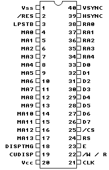
* PIN ARRANGEMENT

* ORDERING INFORMATION

CRTC Bus Timing CRT Display Timing
HD6845S 1.0 Mhz 3.7 Mhz max
HD68A45S 1.5 Mhz
HD68B45S 2.0 Mhz
HD6845R 1.0 Mhz 3.0 Mhz max
HD68A45R 1.5 Mhz
HD68B45R 2.0 Mhz

* ABSOLUTE MAXIMUM RATINGS

* RECOMMENDED OPERATING CONDITIONS

Figure 5 Test Loads

* SYSTEM DESCRIPTION

The CRTC is a LSI which is connected with MPU and CRT display device to control CRT display. The CRTC consists of internal register group, horizontal and vertical timing circuits, linear address generator, cursor control circuit, and light pen detection circuit. Horizontal and vertical timing curcuit generate RA0-RA4, DISPTMG, HSYNC and VSYNC. RA0-RA4 are raster address signals and uses as input signals for Character Generator. DISPTMG, HSYNC and VSYNC signals are recieved by video control circuit. This horizontal and vertical timing circuit consists of internal counter and comparator circuit.

Linear address generates refresh memory address MA0-MA13 to be used for refreshing the screen. By these address signals, refresh memory is accessed periodically. As 14 refresh memory address signals are prepared, 16k words max are accessible. Moreover, the use of start address register enables paging and scrolling. Light pen detection circuit detects light pen position on the screen. When light pen strobe signal is received, light pen register memorizes linar address generated by linear address generator in order to memorize where light pen is on the screen. Cursor control circuit controls the position of cursor, its height, and its blink.

Figure 6 Internal Block Diagram of CRTC

* FUNCTION OF SIGNAL LINE

The CRTC provides 13 interface signals to MPU and 25 interface signals to CRT display.

* Interface Signals to MPU

Bi-directional Data Bus (D0-D7)

I/O Pin No. 33-26

Bi-directional data bus (D0-D7) are used for data transfer between the CRTC and MPU. The data bus outputs are 3-state buffers and remain the high-impedance state except when MPU performs a CRTC read operation.

Read/Write /W / R

Input Pin No.22

Read/Write signal (/W / R) controls the direction of data transfer between the CRTC and MPU. When /W / R is at "High" level, data of CRTC is transferred to MPU. When /W / R is at "low" level, data of MPU is transferred to CRTC.

Chip Select (/CS)

Input Pin No. 25

Chip Select signal (/CS) is used to address the CRTC. When /CS is at a "low" level, it enables Read/Write operation in CRTC internal registers. Normally this signal is derived from decoding address signal of MPU under the condition that VMA of MPU is at "High" level.

Register Select

Input Pin No. 24

Register Select signal (RS) is used to select the address register and 18 control registers of the CRTC. When RS is at "low" level, the address register is selected and when RS is at "high" level, control registers are selected. This signal is normally a derivative of the lowest bit (A0) of MPU address bus.

Enable (E)

Input Pin No. 23

Enable signal (E) is used as strobe signal in MPU Read/Write operation with the CRTC internal registers. This signal is normally a derivative of the HD6800 System Ø, clock.

Reset (/RES)

Reset Signal (/RES) is an input signal used to reset the CRTC. When /RES is at "low" level, it forces the CRTC into the following status: This signal is different from other HD6800 family LSIs in the following functions and has restrictions for usage:

* Interface Signals to CRT Display Device

Character Clock (CLK)

Input Pin No. 21

CLK is a standard clock input signal which defines character timing for the CRT display operation. CLK is normally derived from the external high-speed dot timing logic.

Horizontal Sync (HSYNC)

Output Pin No. 39

HSYNC is an active "high" level signal which provides horizontal syncronization for display device.

Vertical Sync (VSYNC)

Output Pin No. 40

VSYNC is an active "high" level signal which provides vertical sychronization for display device.

Display Timing (DISPTMG)

Output Pin No. 18

DISPTMG is an active "High" level signal which defines the display period in horizontal and vertical raster scanning. It is necessary to enable video signal only when DISPTMG is at "High" level.

Refresh Memory Address (MA0-MA13)

Output Pin. No 4-17

MA0-MA13 are refresh memory address signals which are used to access to refresh memory in order to refresh the CRT screen periodically. These outputs enables 16k words max, refresh memory access. So, for instance, these are applicable to up to 2000 characters/screen and 8-page system.

Raster Address RA0-RA4

Output Pin No. 38-34

RA0-RA4 are raster address signals which are used to select the raster of the character generator or graphic pattern generator etc.

Cursor Display (CUDISP)

Output Pin No. 19

CUDISP is a active "High" level video signal which is used to display the cursor on the CRT screen. This output is inhibited while DISPTMG is at "low" level. Normally this output is mixed with video signal and provided to the CRT display device.

Light Pen Strobe (LPSTB)

Input pin no.3

LPSTB is an "active" level input signal which accepts strobe pulse detected by the light pen and control circuit. When this signal is activated, the refresh memory address (MA0-MA13) which are shown in Fig. 2 are stored in the 14-bit light pen register. The stored refresh memory address need to be corrected in software, taking the delay time of he display device, light pen and light pen control circuits into account.

* REGISTER DESCRIPTION


Table 1 Internal Registers Assignment
/CS RS Address Register Register # Register Name Program Unit READ WRITE Data Bit
4 3 2 1 0 7 6 5 4 3 2 1 0
1 x xxxxx - - -
0 0 xxxxx AR Address Register - X O
0 1 00000 R0 Horizontal Total* Character X O
0 1 00001 R1 Horizontal Displayed Character X O
0 1 00010 R2 Horizontal Sync Position* Character X O
0 1 00011 R3 Sync Width Vertical-Raster, Horizontal-Character X O wv3 wv2 wv1 wv0 wh3 wh2 wh1 wh0
0 1 00100 R4 Vertical Total* Line X O
0 1 00101 R5 Vertical Total Adjust Raster X O
0 1 00110 R6 Vertical Displayed Line X O
0 1 00111 R7 Vertical Sync Position* Line X O
0 1 01000 R8 Interlace and Skew - X O c1 c0 d1 d0 v s
0 1 01001 R9 Maximum Raster Address Raster X O
0 1 01010 R10 Cursor Start Raster Raster X O B P
0 1 01011 R11 Cursor End Raster Raster X O
0 1 01100 R12 Start Address (H) - O O
0 1 01101 R13 Start Address (L) - O O
0 1 01110 R14 Cursor (H) - O O
0 1 01111 R15 Cursor (L) - O O
0 1 10000 R16 Light Pen (H) - O X
0 1 10001 R17 Light Pen (L) - O X


NOTE

* FUNCTION OF INTERNAL REGISTERS

* Address Register (AR)

This is a 5-bit register used to select 18 internal control registers (R0--R17). Its contents are the address of one of 18 internal control registers. Programming the data from 18 to 31 produces no results. Access to R0--R17 requires, first of all, to write the address of corresponding control register into this register. When RS and /CS are at "low" level, this register is selected.

* Horizontal Total Register (R0)

This is a register used to program total number of horizontal characters per line including the retrace period. The data is 8-bit and its value should be programmed according to the specification of the CRT. When M is total number of characters, M-1 shall be programmed to this register. When programming for interlace mode, M must be even.

* Horizontal Displayed Register (R1)

This is a register used to program the number of horizontal displayed characters per line. Data is 8-bit and any number that is smaller than that of horizontal total characters can be programmed.

* Horizontal Sync Position Register (R2)

This is a register used to program horizontal sync position as multiples of the character clock period. Data is 8-bit and any number that is lower than the horizontal total number can be programmed. When H is character number of horizontal Sync Position, H-1 shall be programmed to this register. When programmed value of this register is increased, the display position on the CRT screen is shifted to the left. When programmed value is decreased, the position is shifted to the right. Therefore, the optimum horizontal position can be determined by this value.

* Sync Width Register (R3)

This is a register used to program the horizontal sync pulse width and the vertical sync pulse width. The horizontal sync pulse width is programmed in the lower 4-bits as multiples of the character clock period. "0" can't be programmed. The vertical sync width is programmed in higher 4-bit as multiples of the raster period. When "0" is programmed in higher 4-bit, 16 raster period (16H) is specified.

Table 2: Pulse Width of Vertical Sync Signal
VSW Pulse Width
2^7 2^6 2^5 2^4
0 0 0 0 16H
0 0 0 1 1
0 0 1 0 2
0 0 1 1 3
0 1 0 0 4
0 1 0 1 5
0 1 1 0 6
0 1 1 1 7
1 0 0 0 8
1 0 0 1 9
1 0 1 0 10
1 0 1 1 11
1 1 0 0 12
1 1 0 1 13
1 1 1 0 14
1 1 1 1 15
H; Raster Period


Table 3 Pulse Width of Horizontal Sync Signal
HSW Pulse Width
2^3 2^2 2^1 2^0
0 0 0 0 - (Note)
0 0 0 1 1 CH
0 0 1 0 2
0 0 1 1 3
0 1 0 0 4
0 1 0 1 5
0 1 1 0 6
0 1 1 1 7
1 0 0 0 8
1 0 0 1 9
1 0 1 0 10
1 0 1 1 11
1 1 0 0 12
1 1 0 1 13
1 1 1 0 14
1 1 1 1 15
CH; Character clock period
(Note) HSW = "0" can't be used

* Vertical Total Register (R4)

This is a register used to program total number of lines per frame including vertical retrace period. The data is within 7-bit and its value should be programmed according to the specification of the CRTC. When N is total number of lines, N-1 shall be programmed to this register.

* Vertical Total Adjust Register (R5)

This is a register used to program the optimum number to adjust total number of rasters per field. This register enables to decide the number of vertical deflection frequency more strictly.

* Vertical Displayed Register (R6)

This is a register used to program the number of displayed character rows on the CRT screen. Data is 7-bit and any number that is smaller than that of vertical total characters can be programmed.

* Vertical Sync Position Register (R7)

This is a register used to program the vertical sync position on the screen as multiples of the horizontal character line period. Data is 7-bit and any number that is equal to or less than vertical total characters can be programmed. When V is character number of vertical sync position, V-1 shall be programmed to this register. When programmed value of this register is increased, the display position is shifted up. When programmed value is decreased, the position is shifted down. Therefore, the optimum vertical position may be determined by this value.

* Interlace and Skew Register (R8)

This is a register used to program raster scan mode and skew (delay) of CUDISP and DISPTMG.

Raster Scan Mode Program Bit (V,S)

Raster scan mode is programmed in the V,S bit.

Table 4 Raster Scan Mode (2^1,2^0)
V S Raster Scan Mode
00Non-interlace mode
10
01Interlace Sync Mode
11Interlace Sync & Video Mode


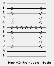
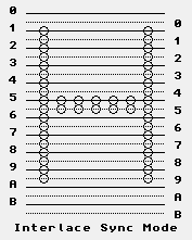
In the non-interlace mode, the rasters of even number field and odd number field are scanned duplicatedly. In the interlace sync mode, the rasters of odd number field are scanned in the middle of even number field. Then it is controlled to display the same character position in two fields. In the interlace sync & video mode, the raster scan method is the same as the interlace sync mode, but it is controlled to display different character pattern in two field.

Skew Program Bit (C1,C0,D1,D0)

These are used to program the skew (delay) of CUDISP and DISPTMG. Skew of these two kinds of signals are programmed seperatly.

Table 5 DISPTMG Skew bit (2^5,2^4)
D1 D0 DISPTMG
00Non-Skew
01One-character Skew
10Two-character skew
11Non-output


Table 6 CUDISP Skew Bit (2^7,2^6)
C1 C0 CUDISP
00Non-Skew
01One-character Skew
10Two-character skew
11Non-output


Skew function is used to delay the output timing of CUDISP and DISPTMG in LSI for he time to access refresh memory, character generator or pattern generator, and to make the same phase with serial video signal.

* Maximum Raster Address Register (R9)

(See comparison of HD6845S and HD6845R on page 40.

This is a register used to program maximum raster address within 5-bit. This register defines total number of rasters per character including line space. This register is programmed as follows.

Non-Interlace mode, Interlace Sync Mode

When total number of rasters is RN, RN-1 shall be programmed.

Interlace Sync & Video Mode

When total number of rasters is RN, RN-2 shall be programmed.

This manual defines total number of rasters in non-interlace mode, interlace sync mode and interlace sync & video mode as follows:
Non-Interlace Mode

0 ------------	  Total Number of rasters: 5
1 ------------    Programmed value: Nr=4
2 ------------    (The same as displayed total number of rasters)
3 ------------
4 ------------
Raster address

Interlace Sync Mode

0 ------------    Total Number of Rasters: 5
  ............ 0  Programmed value: Nr=4
1 ------------    (In the interlace sync mode, total number of rasters
  ............ 1   in both the even and odd fields is ten. On programming,
2 ------------     the half of it is defined as total number of rasters.)
  ............ 2
3 ------------
  ............ 3
4 ------------ 
  ............ 4
Raster address

Interlace Sync & Video Mode

0 ------------    Total number of Rasters: 5
  ............ 1  Programmed Value: Nr=3
2 ------------    (Total number of rasters displayed in the even field
  ............ 3   and the odd field).
4 ------------

* Cursor Start Raster Register (R10)

This is a register used to program the cursor start raster address by the lower 5-bit (2^0--2^4) and the cursor display mode by higher 2-bit. (2^5,2^6)

Table 7 Cursor Display Mode (2^6, 2^5)
B P Cursor Display Mode
00Non-blink
01Cursor-non-display
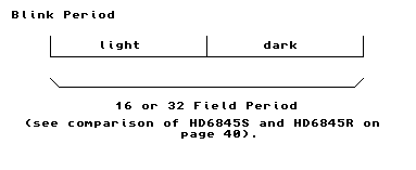
10Blink 16 Field Period
11Blink 32 Field Period


* Cursor End Raster Register (R11)

Tbis is register used to program the cursor end raster address.

* Start Address Register (R12, R13)

These are used to program the first address of refresh memory to read out. Paging and scrolling is easily performed using this register. The register can be read but the higher 2-bit (2^6, 2^7) of R12 are always "0".

* Cursor Register (R14,R15)

These tow read/write registers stores he cursor location. The higher 2-bit (2^6, 2^7) of R14 are always "0".

* Light Pen Register (R16,R17)

These read only registers are used to catch the detection address of the light pen. The higher 2-bit (2^6, 2^7) of R16 are always "0". Its value needs to be corrected by software because there is time delay from address output of the CRTC to signal input LPSTB pin of the CRTC in the process that raster is 1H after address output and ligh pen detects it. Moreover, delay time shown in Fig 2 needs to be taken into account.

Restriction on Programming Internal Register * In the interlace mode, pulse width is changed ±½ raster time when vertical sync signal extends over two fields.

Notes for Use

The method of directly using the value programmed in the internal registers of LSI for controlling the CRT is adopted. Consequently, the display may flicker on the screen when the contents of the registers are changed from bus side asynchonously with the display operation.

Cursor Register

Writing into this register at frequent intervals for moving the cursor should be performed during horizontal and vertical retrace period.

Start Address Register

Writing into the start address register at frequent intervals for scrolling and paging should be performed during horizontal and vertical display period. It is desireable to avoid programming other registers during display operation.

* OPERATION OF THE CRTC

* Time Chart of CRT interface signals

The following example shows the display operation in which values of Table 8 are programmed to the CRTC internal registers. Fig 7 shows the CRT screen format. Fig 10 shows the time chart of signals output from the CRTC.

Figure 7 CRT Screen Format


Table 8 Programmed Values into the Registers
Register Register Name Value Register Register Name Value
R0 Horizontal Total Nht R9 Max Raster Address Nr
R1 Horizontal Displayed Nhd R10 Cursor Start Raster
R2 Horizontal Sync Position Nhsp R11 Cursor End Raster
R3 Sync Width Nvsw,Nhsw R12 Start Address (H) 0
R4 Vertical Total Nvt R13 Start Address (L) 0
R5 Vertical Total Adjust Nadj R14 Cursor (H)
R6 Vertical Displayed Nvd R15 Cursor (L)
R7 Vertical Sync Position Nvsp R16 Light Pen (H)
R8 Interlace & Skew R17 Light Pen (L)
Note: Nhd<Nht, Nvd<Nvt
The relation between values of Refresh Memory Address (MA0-MA13) and Raster Address (RA0-RA7) and the display position on the screen is shown in Fig 16. Fig 16 shows the case where the value of Start Address is 0.

Interlace Control

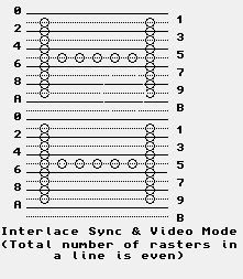
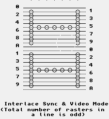
Fig. 8 shows an example where the same character is displayed in the non-interlace mode, interlace sync mode, and interlace sync & video mode.

Non-Interlace Mode Control

In non-interlace mode, each field is scanned dupicatedly. The values of raster address (RA0-RA4) are counted up one from 0.

Interlace Sync Mode Control

In the interlace sync mode, raster addressed in the even field and the odd field are the same as addressed in the non-interlace mode. One character pattern is displayed mutually and its display position in the odd field is set to ½ raster space down from that in the even field.

Figure 8. Example of Raster Scan Display


Non-interlace Mode

Interlace Sync Mode

Interlace Sync & Video Mode
(Total number of rasters in a line is even)

Interlace Sync & Video Mode
(Total number of rasters in a line is odd.)

Interlace Sync & Video Mode Control

In interlace sync and video mode, the output raster address when the number of rasters is even is different from that when the number of rasters is odd.

Table 9 The Output Of Raster Address in Interlace Sync & Video Mode
Total number of Rasters in a Line Field Even Field Odd Field
Even Even Address Odd Address
Odd Even Line * Even Address Odd Address
Odd Line * Odd Address Even Address
* Internal line address begins from 0.


Cursor Control

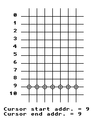
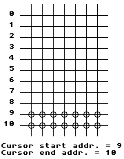
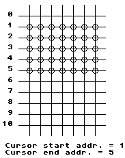
Fig 9 show the display patterns where each value is programmed to the cursor start raster register and the cursor end raster register. Programmed values to the cursor start raster register and the cursor end raster register need to be under the following condition.

Cursor Start Raster Register<=Cursor End Raster Register<=Maximum Raster Address Register.

Time chart of CUDISP is shown in Fig 14 and Fig 15.

Figure 9 Cursor Control

Figure 10 CRTC Time Chart

Figure 12 Fine Adjustment Period of Frame in Vertical Display
(Expansion of fig 10 - R

Figure 13 Interlace Control

Figure 15 CUDISP Timing (Expansion of Fig 14. C

Figure 16 Refresh Memory Address (MA0--MA13

* How to use the CRTC

* DISPLAY SEQUENCE AFTER /RES REKEASE OF HD6845S

HD6845S starts the display operation immediatly after the release of /RES. The operation at the first field is different from the normal subsequent display operation.

[Operation at the first field after the /RES release]

Figure 42 /RES Release sequence

Figure 43 Release sequence in the Non-Interlace Mode

Figure 44 Release sequence in the Interlace Mode (1)

Figure 44 Release sequence in the Interlace Mode (2)

* ANOMALOUS OPERATIONS IN HD6845S CAUSED BY REWRITING REGISTERS DURING DISPLAY OPERATION *


Register # Register Name Anomalous opeations caused by rewriting registers & Conditions to avoid those operations Rewriting** OK or NG
R0 Horizontal Total The horizontal scan period is disturbed. X
R1 Horizontal Displayed There are some cases where the width of DISPTMG becomes shorter than the programmed value at the moment of the rewrite operation. An error operation occurs only during one raster period. O
R2 Horizontal Sync Position There are some cases where HSYNC is placed on the position different from the programmed value or the noise is output. X
R3 Sync Width When a rewrite operation is performed at a "High" level on HSYNC pulse or VSYNC pulse, there are some cases where the width pulse becomes shorter than the programmed value at the moment of a rewrite operation. /\
R4 Vertical Total When a rewrite operation is performed during the last raster period in the line, there is a possibility that the disturbance occurs during the vertical scan period. There is no problem of a rewrite operation during raster period except this period. /\
R5 Vertical Total Adjust When a rewrite operation is performed in the last character time of the raster period, there are some cases where the numbers of Adjust Register, specified by program, are not added. (Only during the adjust raster period). /\
R6 Vertical Displayed After the moment of a rewrite operation, there are some cases where the Display is inhibited. However, the display according to the programmed value is performed from the next field. O
R7 Vertical Sync Position There are some cases where VSYNC is placed on the position different from the programmed value or the noise is output. X
R8 Interlace & Skew Neither scan mode bit nor skew bit is rewritten dynamically. Dynamic Rewrite into scan mode bit and skew bit is prohibited. X
R9 Maximum Raster Address The internal operation will be disordered by a rewrite operation. X
R10 Cursor Start Raster When a rewrite operation is performed in the last character time of the raster period, there are some cases where the jitter occurs on the cursor raster or the cursor is not displayed correctly. There is also a possibility that the blink rate becomes temporarily shorter than usual. /\
R11 Cursor End Raster When a rewrite operation is performed in the last character time of the raster period, there are some cases where the jitter occurs on the cursor rraster or the cursor is not displayed correctly. Moreover, there are also some cases where the blink rate becomes temporarily shorter than normal operation. /\
R12 Start Address (H) R12 and R13 are used in the last raster period of the field. A rewrite operation can be performed except during this period. However, when R12 and R13 are rewritten in each field seperatly, the display operation, whose start address is determined temporarily by programming sequence, will be performed. A rewrite operation should be performed during the horizontal/vertical display period. O
R13 Start Address (L) O
R14 Cursor (H) When a rewrite operation is performed during the display period, there are some cases where the cursor is temporarily displayed at the address different from the programmed value. A rewrite operation should be performed during the horizontal/vertical retrace period. Also, when R14 and R15 are rewritten in each field seperatly, the cursor is displayed temporarily at the temporal address by programming sequence. O
R15 Cursor (L) O


COMPARISON BETWEEN HD6845S AND HD6845R

Comparison of function between HD6845S and HD6845R

No. Functional Difference HD6845R HD6845S
1 Interlace Sync & Video Mode Display Programming Method of Number of Vertical Characters In HD6845R, number of characters is vertically programmed in a unit of two lines, as illustrated above. (Number of vertical total characters, Number of vertical displayed characters, Vertical Sync Position).

Example of above figure

Programmed number into Vertical Display Register = 5
In HD6845S, number of characters is vertically programmed in a unit of one lines, as illustrated above. (Number of vertical total characters, Number of vertical displayed characters, Vertical Sync Position).

Example of above figure

Programmed number into Vertical Display Register = 10
Number of Rasters per Character Line Only even number can be specified. Both even and odd number can be specified
Number of raster = 10 scan-line (specified) When number of raster per character line is EVEN. Number of raster = 10 scan line (specified) When number of raster per character line is ODD. Number of raster = 9 scan line (specified)
However, number which is programmed into register is calculated as follows.

Programmed number (Nr) = (Number specified)-1
However, number which is programmed into register is calculated as follows:

Programmed number (Nr) = (Number specified-2)
Cursor Display Cursor is displayed in either EVEN field or ODD field
[Example 1]


[Example 2]
Cursor is displayed in both EVEN and ODD field
[Example 1]


[Example 2]


[Example 3]
2 Vertical Sync Pulse Width (VSYNC output) Fixed at 16 raster scan cycle (16H) Programmable (1-16 raster scan cycle
3 SKEW function Not included SKEW function is newly included in DISPTMG, CUDISP signals
4 Start Address Register Impossible to READ Possible to READ
5 RESET signal (/RES) MA0-MA13 Output, RA0-RA4 - Synchronous Reset
Other Outputs - Asynchronous Reset

Output signals of MA0-MA13, RA0-RA4 synchronising with DLK "low" level, go to "low" level after /RES has gone to "low". Other outputs go to "low" immediatly after /RES has gone to "low"level.
MA0-MA13 Output, RA0-RA4, Other Outputs - Asynchronous Reset

Output signals of MA0-MA13, RA0-RA4 and others go to "low" level immediatly after /RES has gone to "low" level.

COMPATIBILITY OF HD6845S AND HD6845R

Non-interlace Mode Fully compatible with HD6845R (note 1). HD6845R can be directly replaced by HD6845S in these modes.
Interlace Sync Mode
Interlace sync & Video mode control Not compatible with HD6845R in regard to programming and data for vertical direction need to be changed.