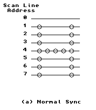
(a) Normal Sync
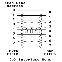
(b) Interlace Sync
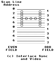
(c) Interlace Sync and Video
| Rating | Symbol | Value | Unit |
|---|---|---|---|
| Supply Voltage | Vcc | -0.3 to 7.0 | V |
| Input Voltage | Vin | -0.3 to 7.0 | V |
| Operating Temperature Range | TA | Tl to Th | °C |
| MC6845,MC68A45, MC68B45 | 0 to 70 | ||
| MC6845C, MC68A45C | -40 to +85 | ||
| Storage Temperature Range | Tstg | -55 to 150 | °C |
| Characteristics | Symbol | Value | Unit |
|---|---|---|---|
| 0JA | CW | ||
| Plastic Package | 100 | ||
| Cerdip Package | 60 |
| Characteristics | Symbol | Min. | Typ. | Max. | Unit |
|---|---|---|---|---|---|
| Supply Voltage | Vcc | 4.75 | 5.0 | 5.25 | V |
| Input Low Voltage | Vil | -0.3 | - | 0.8 | |
| Input High Voltage | Vih | 2.0 | - | Vcc |
| Characteristics | Symbol | Min. | Typ. | Max. | Units | |
|---|---|---|---|---|---|---|
| Input High Voltage | VIH | 2.0 | - | Vcc | V | |
| Input Low Voltage | VIL | -0.3 | 0.8 | V | ||
| Input Leakage Current | IIN | - | 0.1 | 2.5 | uA | |
| Hi-Z State Input Current (Vcc=5.25 V) VIN = 0.4 to 2.4V | ITSI | -10/td> | - | 10 | uA | |
| Output High Voltage | VOH | V | ||||
| (ILOAD = -205 uA) D0-D7 | 2.4 | 3.0 | - | |||
| (ILOAD = -100 uA) Other outputs | 2.4 | 3.0 | - | |||
| Output Low Voltage ILOAD = 1.6mA |
VOL | - | 0.3 | 0.4 | V | |
| Internal Power Dissipation (Measured at Ta=0C) | PINT | - | 600 | 750 | mW | |
| Input Capacitance | CIN | pF | ||||
| D0-D7 | - | - | 12.5 | |||
| All Others | - | - | 10 | |||
| Output Capacitance | COUT | - | - | 10 | pF | |
| Ident. Number | Characteristics | Symbol | MC6845 | MC68A45 | MC68B45 | Units | |||
|---|---|---|---|---|---|---|---|---|---|
| Min. | Max. | Min. | Max. | Min. | Max. | ||||
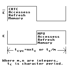
| 1 | Cycle Time | tCYC | 1.0 | 10** | 0.67 | 10 | 0.5 | 10** | us |
| 2 | E Pulse Width, Low | PWEL | 430 | - | 280 | - | 210 | - | ns |
| 3 | PWEH | E Pulse Width, High | 450 | - | 280 | - | 220 | - | ns |
| 4 | Clock Rise and Fall Time | tr,tf | - | 25 | - | 25 | - | 20 | ns |
| 9 | Address Hold Time | tAH | 10 | - | 10 | - | 10 | - | ns |
| 13 | RS Setup Time Before E | tAS | 80 | - | 60 | - | 40 | - | ns |
| 14 | /W/R, /CS Set-Up Time Before E | tCS | 80 | - | 60 | - | 40 | - | ns |
| 15 | /W/R, /CS Hold Time | tCH | 10 | - | 10 | - | 10 | - | ns |
| 18 | Read Data Hold Time | tDHR | 20 | 50* | 20 | 50* | 20 | 50* | ns |
| 21 | Write Data Hold Time | tDHW | 10 | - | 10 | - | 10 | - | ns |
| 30 | Peripheral Output Data Delay Time | tDDR | - | 290 | - | 180 | 0 | 150 | ns |
| 31 | Peripheral Input Data Delay Time | tDSW | 165 | - | 80 | - | 60 | ns | |
| Characteristic | Symbol | Min. | Max. | Units |
|---|---|---|---|---|
| Maximum Clock Pulse Width, Low | PWCL | 150 | - | ns |
| Maximum Clock Pulse Width, High | PWCH | 150 | - | ns |
| Clock Frequency | fc | - | 3.0 | Mhz |
| Rise and Fall Time for Clock Input | Tcr,Tcf | - | 20 | ns |
| Memory Address Delay Time | tMAD | - | 160 | ns |
| Raster Address Delay Time | tRAD | - | 160 | ns |
| Display Timing Delay Time | tDTD | - | 250 | ns |
| Horizontal Sync Delay Time | tHSD | - | 250 | ns |
| Vertical Sync Delay Time | tVSD | - | 250 | ns |
| Cursor Display Timing Delay Time | tCDD | - | 250 | ns |
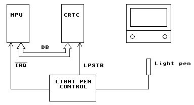
| Light Pen Strobe Maximum Pulse Width | PWLPH | 80 | - | ns |
| Light Pen Strobe Disable Time | tLPD1 | - | 80 | ns |
| tLPD2 | - | 10 | ns |
| /RESET | /LPSTB | Operating Mode |
|---|---|---|
| 0 | 0 | Reset |
| 0 | 1 | Test Mode |
| 1 | 0 | Normal Mode |
| 1 | 1 | Normal Mode |
| /CS | RS | Address Register | Register # | Register File | Program Unit | READ | WRITE | Number of bits | |||||||||||
|---|---|---|---|---|---|---|---|---|---|---|---|---|---|---|---|---|---|---|---|
| 4 | 3 | 2 | 1 | 0 | 7 | 6 | 5 | 4 | 3 | 2 | 1 | 0 | |||||||
| 1 | x | x | x | x | x | x | x | - | - | - | - | ||||||||
| 0 | 0 | x | x | x | x | x | AR | Address Register | - | No | Yes | ||||||||
| 0 | 1 | 0 | 0 | 0 | 0 | 0 | R0 | Horizontal Total | Char | No | Yes | ||||||||
| 0 | 1 | 0 | 0 | 0 | 0 | 1 | R1 | Horizontal Displayed | Char | No | Yes | ||||||||
| 0 | 1 | 0 | 0 | 0 | 1 | 0 | R2 | H. Sync Position | Char | No | Yes | ||||||||
| 0 | 1 | 0 | 0 | 0 | 1 | 1 | R3 | Sync Width | - | No | Yes | wv3 | H | H | H | H | |||
| 0 | 1 | 0 | 0 | 1 | 0 | 0 | R4 | Vertical Total | Char row | No | Yes | ||||||||
| 0 | 1 | 0 | 0 | 1 | 0 | 1 | R5 | V. Total Adjust | Scan line | No | Yes | ||||||||
| 0 | 1 | 0 | 0 | 1 | 1 | 0 | R6 | Vertical Displayed | Char row | No | Yes | ||||||||
| 0 | 1 | 0 | 0 | 1 | 1 | 1 | R7 | V. Sync Position | Char row | No | Yes | ||||||||
| 0 | 1 | 0 | 1 | 0 | 0 | 0 | R8 | Interlace Mode and Skew | Note 1 | No | Yes | I | I | ||||||
| 0 | 1 | 0 | 1 | 0 | 0 | 1 | R9 | Max Scan Line Address | Scan line | No | Yes | ||||||||
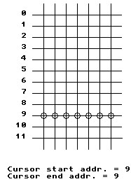
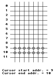
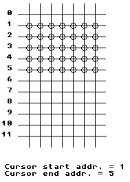
| 0 | 1 | 0 | 1 | 0 | 1 | 0 | R10 | Cursor Start | Scan line | No | Yes | B | P | ||||||
| 0 | 1 | 0 | 1 | 0 | 1 | 1 | R11 | Cursor End | Scan line | No | Yes | ||||||||
| 0 | 1 | 0 | 1 | 1 | 0 | 0 | R12 | Start Address (H) | - | No | Yes | 0 | 0 | ||||||
| 0 | 1 | 0 | 1 | 1 | 0 | 1 | R13 | Start Address (L) | - | No | Yes | ||||||||
| 0 | 1 | 0 | 1 | 1 | 1 | 0 | R14 | Cursor (H) | - | Yes | Yes | 0 | 0 | ||||||
| 0 | 1 | 0 | 1 | 1 | 1 | 1 | R15 | Cursor (L) | - | Yes | Yes | ||||||||
| 0 | 1 | 1 | 0 | 0 | 0 | 0 | R16 | Light Pen (H) | - | Yes | No | 0 | 0 | ||||||
| 0 | 1 | 1 | 0 | 0 | 0 | 1 | R17 | Light Pen (L) | - | Yes | No | ||||||||
| Bit 1 | Bit 0 | Mode |
|---|---|---|
| 0 | 0 | Normal Sync Mode (Non-Interlaced) |
| 1 | 0 | |
| 0 | 1 | Interlace Sync Mode |
| 1 | 1 | Interlace Sync and Video Mode |
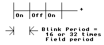
| Bit 6 | Bit 5 | Cursor Display Mode |
|---|---|---|
| 0 | 0 | Non-Blink |
| 0 | 1 | Cursor Non-Display |
| 1 | 0 | Blink, 1/16 field rate |
| 1 | 1 | Blink, 1/32 field rate |
| Reg. # | Register Name | Value | Programmed Value |
|---|---|---|---|
| R0 | H. Total | Nht + 1 | Nht |
| R1 | H. Displayed | Nhd | Nhd |
| R2 | H. Sync Position | Nhsp | Nhsp |
| R3 | H. Sync Width | Nhsw | Nhsw |
| R4 | V. Total | Nvt + 1 | Nvt |
| R5 | V. Scan Line Adjust | Nadj | Nadj |
| R6 | V. Displayed | Nvd | Nvd |
| R7 | V.Sync Position | Nvsp | Nvsp |
| R8 | Interlace Mode | ||
| R9 | Max Scan Line Address | Nsl | Nsl |
| Register | Name | Contents |
|---|---|---|
| R8 | Interlace Mode Register | See Table 3 |
| R10 | Cursor Start | See Figure 15 and Table 4 |
| R11 | Cursor End | See Figure 15 |
| R12 | Start Address (H) | User programs first memory location to be displayed | R13 | Start Address (L) |
| R14 | Cursor (H) | User programs desired cursor location | R15 | Cursor (L) |
| R16 | Light Pen (H) | Can be loaded via light-pen strobe only |
| R17 | Light Pen (L) |
| Register | Function |
|---|---|
| R0 | Horizontal Total |
| R1 | Horizontal Displayed |
| R2 | Horizontal Sync Position |
| R3 | Horizontal Sync Width |
| R4 | Vertical Total |
| R5 | Vertical Total Adjust |
| R6 | Vertical Displayed |
| R7 | Vertical Sync Position |
| R8 | Interlace Mode |
| R9 | Maximum Scan Line Address |
| R10 | Cursor Start |
| R11 | Cursor End |
| R12 | Start Address (H) |
| R13 | Start Address (L) |
| R14 | Cursor (H) |
| R15 | Cursor (L) |
| R16 | Light Pen (H) |
| R17 | Light Pen (L) |
| Symbol | Description | Calculation |
|---|---|---|
| f' | Dot Frequency (1st approx) | (B5×(B7+B9))÷((1÷B1)-B3) |
| tc | Character time | 1÷([(R0)+1]×B1 |
| f | Dot frequency | (B7+B9)÷tc |
| ts | Scan line time | [(R0)+1]×tc |
| n | Total # of scan lines | 1÷(B2×tsl) |
| N | Integer | (n÷(B8+B10)) = N + (R÷(B8+B10)) |
| R | Integer Remainder | |
| tcr | Character row time | (B8+B10)×tsl |
| thr | Horizontal retrace time | <= ([(R0)+1-B5]×(B7+B9))/f |
| tvr | Vertical retrace time | <= (B1÷B2) - (B6(B8+B10)×tsl) |
| Register | Calculation |
|---|---|
| R0 | (f'÷(B1×(B7+B9))-1 |
| R1 | B5 |
| R2 | (R1) + ((R3)÷R2) |
| R3 | ((R0) - (R1))÷3 |
| R4 | N-1 |
| R5 | R |
| R6 | B6 |
| R7 | [(R4)+1] - ((16 - (R5))÷(B8+B10) >= (R7) >= (R6) |
| R9 | (B8 + B10)-1 |
| Package Type | Frequency Mhz | Temperature | Order number |
|---|---|---|---|
| Cerdip S suffix | 1.0 | 0°C to 70°C | MC6845S |
| 1.0 | -40°C to -85°C | MC6845CS | |
| 1.5 | 0°C to 70°C | MC68A45S | |
| 1.5 | -40°C to +85°C | MC68A45CS | |
| 2.0 | 0°C to 70°C | MC68B45S | |
| Plastic P suffix | 1.0 | 0°C to 70°C | MC6845P |
| 1.0 | -40°C to -85°C | MC6845CP | |
| 1.5 | 0°C to 70°C | MC68A45P | |
| 1.5 | -40°C to +85°C | MC68A45CP | |
| 2.0 | 0°C to 70°C | MC68B45P |